Solving for Adhesive Needs in Microchip Applications
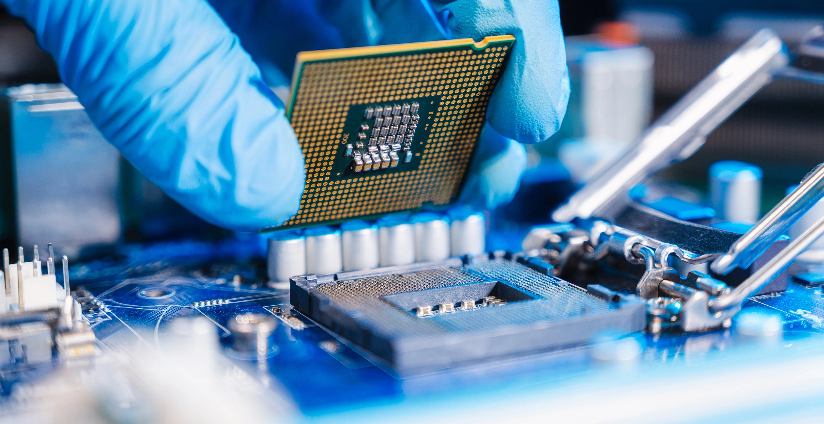
The electronic devices manufactured today are increasingly reliant upon miniature chip technology. This use of miniature electronic components is spanning industries. For example, in the automotive industry, the average car is projected to contain $500 USD worth of microchips in 2022, totaling a value of more than $60 billion for microchips in the automotive industry. In the healthcare industry, the use of chips is also growing as more healthcare devices, such as watches and smart patches, rise in popularity due to the growth of telehealth. In addition, the use of chips for machine learning training and artificial intelligence applications is projected to grow more than 50% annually across every computing category.
As more devices across industries necessitate the use of chips, manufacturers face a unique challenge. Chips that were once soldered into place in large computer frames are now added to increasingly small devices. In addition, cameras, smartphones, and wearable devices all require the miniaturization of chips, which increases the difficulty of soldering.
Seeing the need for improved soldering processes, one of our group companies, PacTech, recently took on the challenge, looking for a solution that would meet the needs of our customers.
The Challenge
Working with technicians across industries, our group first identified the challenges of the miniaturization of electronic components. The challenges we sought to solve included the following:
- How to handle the difficulty of soldering as the size of components becomes increasingly minute
- How to mount solder balls without the use of flux, an acidic mixture that can cause electronic failures
- How to mount solder balls when they cannot be mounted on the pinpoint
- How to accurately solder when the shape is complicated and how to integrate parts when solder mounting below 100 μm is not possible
The Solution
Looking at the complexity of these issues, we determined that by utilizing the PacTech’s specialized soldering equipment, it is possible to accurately mount the solder ball on the target, even in the case of a minute chip.
The Process
Using PacTech’s equipment, individual solder balls were sent from a solder ball tank to a capillary, where they waited at the tip of the capillary. A laser was used to melt the solder ball in the capillary, allowing the solder to be accurately shot onto the target pad on the board.
To determine whether or not our equipment solution would hold up to actual customer needs, we used a prototype to check whether the solder could be mounted on customer-designed boards. Additionally, through the testing process, we verified whether or not the solder could be applied to the substrates desired by our customers.
The Results
The laser reflow method that we utilized, which does not use flux, provides accurate solder bumps regardless of the solder material. Traditional methods that employ flux require many liters of water to clean the flux, negatively impacting the environment. Since our process is fluxless, chemical-free, and requires no cleaning, it is environmentally friendly and reduces the total cost of production.
Additionally, since maskless solder can be supplied and mounted, manufacturers can reduce environmental concerns and the total production cost.
As a result of using our equipment, soldering to fine chips is now possible.
Through our process, the number of solder balls that can be mounted within a fixed time has also been increased by improving the production tact while simultaneously lowering the total cost of production.
Looking Ahead
For industries seeking an improved soldering process for miniature chips, we propose using the equipment designed by PacTech - Packaging Technologies GmbH a NAGASE Group company.
Related Resources
We’re Here to Help
Complete the following fields with your information, as well as a short, detailed description of your request and a NAGASE Specialist will be in touch with you shortly.


